
-
Capacitors
- Ceramic Capacitors
- Tantalum Capacitors
- Accessories
- Aluminum - Polymer Capacitors
- Aluminum Electrolytic Capacitors
- Capacitor Networks, Arrays
- Electric Double Layer Capacitors (EDLC), Supercapacitors
- Film Capacitors
- Mica and PTFE Capacitors
- Niobium Oxide Capacitors
- Silicon Capacitors
- Tantalum - Polymer Capacitors
- Thin Film Capacitors
- Trimmers, Variable Capacitors
-
Discrete Semiconductor Products
- Diodes - Bridge Rectifiers
- Diodes - Rectifiers - Arrays
- Diodes - Rectifiers - Single
- Diodes - RF
- Diodes - Variable Capacitance (Varicaps, Varactors)
- Diodes - Zener - Arrays
- Diodes - Zener - Single
- Power Driver Modules
- Thyristors - DIACs, SIDACs
- Thyristors - SCRs
- Thyristors - SCRs - Modules
- Thyristors - TRIACs
- Transistors - Bipolar (BJT) - Arrays
- Transistors - Bipolar (BJT) - Arrays, Pre-Biased
- Transistors - Bipolar (BJT) - RF
- Transistors - Bipolar (BJT) - Single
- Transistors - Bipolar (BJT) - Single, Pre-Biased
- Transistors - FETs, MOSFETs - Arrays
- Transistors - FETs, MOSFETs - RF
- Transistors - FETs, MOSFETs - Single
- Transistors - IGBTs - Arrays
- Transistors - IGBTs - Modules
- Transistors - IGBTs - Single
- Transistors - JFETs
- Transistors - Programmable Unijunction
- Transistors - Special Purpose
- Inductors, Coils, Chokes
-
Integrated Circuits (ICs)
- Audio Special Purpose
- Clock/Timing - Application Specific
- Clock/Timing - Clock Buffers, Drivers
- Clock/Timing - Clock Generators, PLLs, Frequency Synthesizers
- Clock/Timing - Delay Lines
- Clock/Timing - IC Batteries
- Clock/Timing - Programmable Timers and Oscillators
- Clock/Timing - Real Time Clocks
- Data Acquisition - ADCs/DACs - Special Purpose
- Data Acquisition - Analog Front End (AFE)
- Data Acquisition - Analog to Digital Converters (ADC)
- Data Acquisition - Digital Potentiometers
- Data Acquisition - Digital to Analog Converters (DAC)
- Data Acquisition - Touch Screen Controllers
- Embedded - CPLDs (Complex Programmable Logic Devices)
- Embedded - DSP (Digital Signal Processors)
- Embedded - FPGAs (Field Programmable Gate Array)
- Embedded - FPGAs (Field Programmable Gate Array) with Microcontrollers
- Embedded - Microcontroller or Microprocessor Modules
- Embedded - Microcontrollers
- Embedded - Microcontrollers - Application Specific
- Embedded - Microprocessors
- Embedded - PLDs (Programmable Logic Device)
- Embedded - System On Chip (SoC)
- Interface - Analog Switches - Special Purpose
- Interface - Analog Switches, Multiplexers, Demultiplexers
- Interface - CODECs
- Interface - Controllers
- Interface - Direct Digital Synthesis (DDS)
- Interface - Drivers, Receivers, Transceivers
- Interface - Encoders, Decoders, Converters
- Interface - Filters - Active
- Interface - I/O Expanders
- Interface - Modems - ICs and Modules
- Interface - Modules
- Interface - Sensor and Detector Interfaces
- Interface - Serializers, Deserializers
- Interface - Signal Buffers, Repeaters, Splitters
- Interface - Signal Terminators
- Interface - Specialized
- Interface - Telecom
- Interface - UARTs (Universal Asynchronous Receiver Transmitter)
- Interface - Voice Record and Playback
- Linear - Amplifiers - Audio
- Linear - Amplifiers - Instrumentation, OP Amps, Buffer Amps
- Linear - Amplifiers - Special Purpose
- Linear - Amplifiers - Video Amps and Modules
- Linear - Analog Multipliers, Dividers
- Linear - Comparators
- Linear - Video Processing
- Logic - Buffers, Drivers, Receivers, Transceivers
- Logic - Comparators
- Logic - Counters, Dividers
- Logic - FIFOs Memory
- Logic - Flip Flops
- Logic - Gates and Inverters
- Logic - Gates and Inverters - Multi-Function, Configurable
- Logic - Latches
- Logic - Multivibrators
- Logic - Parity Generators and Checkers
- Logic - Shift Registers
- Logic - Signal Switches, Multiplexers, Decoders
- Logic - Specialty Logic
- Logic - Translators, Level Shifters
- Logic - Universal Bus Functions
- Memory
- Memory - Batteries
- Memory - Configuration Proms for FPGAs
- Memory - Controllers
- PMIC - AC DC Converters, Offline Switchers
- PMIC - Battery Chargers
- PMIC - Battery Management
- PMIC - Current Regulation/Management
- PMIC - Display Drivers
- PMIC - Energy Metering
- PMIC - Full, Half-Bridge Drivers
- PMIC - Gate Drivers
- PMIC - Hot Swap Controllers
- PMIC - Laser Drivers
- PMIC - LED Drivers
- PMIC - Lighting, Ballast Controllers
- PMIC - Motor Drivers, Controllers
- PMIC - OR Controllers, Ideal Diodes
- PMIC - PFC (Power Factor Correction)
- PMIC - Power Distribution Switches, Load Drivers
- PMIC - Power Management - Specialized
- PMIC - Power Over Ethernet (PoE) Controllers
- PMIC - Power Supply Controllers, Monitors
- PMIC - RMS to DC Converters
- PMIC - Supervisors
- PMIC - Thermal Management
- PMIC - V/F and F/V Converters
- PMIC - Voltage Reference
- PMIC - Voltage Regulators - DC DC Switching Controllers
- PMIC - Voltage Regulators - DC DC Switching Regulators
- PMIC - Voltage Regulators - Linear
- PMIC - Voltage Regulators - Linear + Switching
- PMIC - Voltage Regulators - Linear Regulator Controllers
- PMIC - Voltage Regulators - Special Purpose
- Specialized ICs
- Isolators
- Relays
-
RF/IF and RFID
- Attenuators
- Balun
- RF Accessories
- RF Amplifiers
- RF Antennas
- RF Demodulators
- RF Detectors
- RF Diplexers
- RF Directional Coupler
- RF Evaluation and Development Kits, Boards
- RF Front End (LNA + PA)
- RF Misc ICs and Modules
- RF Mixers
- RF Modulators
- RF Power Controller ICs
- RF Power Dividers/Splitters
- RF Receiver, Transmitter, and Transceiver Finished Units
- RF Receivers
- RF Shields
- RF Switches
- RF Transceiver ICs
- RF Transceiver Modules
- RF Transmitters
- RFI and EMI - Contacts, Fingerstock and Gaskets
- RFI and EMI - Shielding and Absorbing Materials
- RFID Accessories
- RFID Antennas
- RFID Evaluation and Development Kits, Boards
- RFID Reader Modules
- RFID Transponders, Tags
- RFID, RF Access, Monitoring ICs
- RF Circulators and Isolators
-
Sensors, Transducers
- Accessories
- Amplifiers
- Capacitive Touch Sensors, Proximity Sensor ICs
- Color Sensors
- Current Transducers
- Dust Sensors
- Encoders
- Flex Sensors
- Float, Level Sensors
- Flow Sensors
- Force Sensors
- Gas Sensors
- Humidity, Moisture Sensors
- Image Sensors, Camera
- IrDA Transceiver Modules
- Magnetic Sensors - Compass, Magnetic Field (Modules)
- Magnetic Sensors - Linear, Compass (ICs)
- Magnetic Sensors - Position, Proximity, Speed (Modules)
- Magnetic Sensors - Switches (Solid State)
- Magnets - Multi Purpose
- Magnets - Sensor Matched
- Motion Sensors - Accelerometers
- Motion Sensors - Gyroscopes
- Motion Sensors - IMUs (Inertial Measurement Units)
- Motion Sensors - Inclinometers
- Motion Sensors - Optical
- Motion Sensors - Tilt Switches
- Motion Sensors - Vibration
- Multifunction
- Optical Sensors - Ambient Light, IR, UV Sensors
- Optical Sensors - Distance Measuring
- Optical Sensors - Mouse
- Optical Sensors - Photo Detectors - CdS Cells
- Optical Sensors - Photo Detectors - Logic Output
- Optical Sensors - Photo Detectors - Remote Receiver
- Optical Sensors - Photodiodes
- Optical Sensors - Photoelectric, Industrial
- Optical Sensors - Photointerrupters - Slot Type - Logic Output
- Optical Sensors - Photointerrupters - Slot Type - Transistor Output
- Optical Sensors - Phototransistors
- Optical Sensors - Reflective - Analog Output
- Optical Sensors - Reflective - Logic Output
- Position Sensors - Angle, Linear Position Measuring
- Pressure Sensors, Transducers
- Proximity Sensors
- Proximity/Occupancy Sensors - Finished Units
- Sensor Cable - Accessories
- Sensor Cable - Assemblies
- Sensor Interface - Junction Blocks
- Shock Sensors
- Solar Cells
- Specialized Sensors
- Strain Gauges
- Temperature Sensors - Analog and Digital Output
- Temperature Sensors - NTC Thermistors
- Temperature Sensors - PTC Thermistors
- Temperature Sensors - RTD (Resistance Temperature Detector)
- Temperature Sensors - Thermocouple, Temperature Probes
- Temperature Sensors - Thermostats - Mechanical
- Temperature Sensors - Thermostats - Solid State
- Ultrasonic Receivers, Transmitters
- Camera Modules
- LVDT Transducers (Linear Variable Differential Transformer)
- Optical Sensors - Photonics - Counters, Detectors, SPCM (Single Photon Counting Module)
- Touch Sensors
-
Circuit Protection
- Accessories
- Circuit Breakers
- Electrical, Specialty Fuses
- Fuseholders
- Fuses
- Gas Discharge Tube Arresters (GDT)
- Ground Fault Circuit Interrupter (GFCI)
- Inrush Current Limiters (ICL)
- Lighting Protection
- PTC Resettable Fuses
- Surge Suppression ICs
- TVS - Diodes
- TVS - Mixed Technology
- TVS - Surge Protection Devices (SPDs)
- TVS - Thyristors
- TVS - Varistors, MOVs
- Thermal Cutoffs (Thermal Fuses)
-
Connectors, Interconnects
- Backplane Connectors - ARINC Inserts
- Backplane Connectors - ARINC
- Backplane Connectors - Accessories
- Backplane Connectors - Contacts
- Backplane Connectors - DIN 41612
- Backplane Connectors - Hard Metric, Standard
- Backplane Connectors - Housings
- Backplane Connectors - Specialized
- Banana and Tip Connectors - Accessories
- Banana and Tip Connectors - Adapters
- Banana and Tip Connectors - Binding Posts
- Banana and Tip Connectors - Jacks, Plugs
- Barrel - Accessories
- Barrel - Adapters
- Barrel - Audio Connectors
- Barrel - Power Connectors
- Between Series Adapters
- Blade Type Power Connectors - Accessories
- Blade Type Power Connectors - Contacts
- Blade Type Power Connectors - Housings
- Blade Type Power Connectors
- Card Edge Connectors - Accessories
- Card Edge Connectors - Adapters
- Card Edge Connectors - Contacts
- Card Edge Connectors - Edgeboard Connectors
- Card Edge Connectors - Housings
- Circular Connectors - Accessories
- Circular Connectors - Adapters
- Circular Connectors - Backshells and Cable Clamps
- Circular Connectors - Contacts
- Circular Connectors - Housings
- Circular Connectors
- Coaxial Connectors (RF) - Accessories
- Coaxial Connectors (RF) - Adapters
- Coaxial Connectors (RF) - Contacts
- Coaxial Connectors (RF) - Terminators
- Coaxial Connectors (RF)
- Contacts - Leadframe
- Contacts - Multi Purpose
- Contacts, Spring Loaded (Pogo Pins), and Pressure
- D-Shaped Connectors - Centronics
- D-Sub Connectors
- D-Sub, D-Shaped Connectors - Accessories - Jackscrews
- D-Sub, D-Shaped Connectors - Accessories
- D-Sub, D-Shaped Connectors - Adapters
- D-Sub, D-Shaped Connectors - Backshells, Hoods
- D-Sub, D-Shaped Connectors - Contacts
- D-Sub, D-Shaped Connectors - Housings
- D-Sub, D-Shaped Connectors - Terminators
- FFC, FPC (Flat Flexible) Connectors - Accessories
- FFC, FPC (Flat Flexible) Connectors - Contacts
- FFC, FPC (Flat Flexible) Connectors - Housings
- FFC, FPC (Flat Flexible) Connectors
- Fiber Optic Connectors - Accessories
- Fiber Optic Connectors - Adapters
- Fiber Optic Connectors - Housings
- Fiber Optic Connectors
- Heavy Duty Connectors - Accessories
- Heavy Duty Connectors - Assemblies
- Heavy Duty Connectors - Contacts
- Heavy Duty Connectors - Frames
- Heavy Duty Connectors - Housings, Hoods, Bases
- Heavy Duty Connectors - Inserts, Modules
- Keystone - Accessories
- Keystone - Faceplates, Frames
- Keystone - Inserts
- LGH Connectors
- Memory Connectors - Accessories
- Memory Connectors - Inline Module Sockets
- Memory Connectors - PC Card Sockets
- Memory Connectors - PC Cards - Adapters
- Modular Connectors - Accessories
- Modular Connectors - Adapters
- Modular Connectors - Jacks With Magnetics
- Modular Connectors - Jacks
- Modular Connectors - Plug Housings
- Modular Connectors - Plugs
- Modular Connectors - Wiring Blocks - Accessories
- Modular Connectors - Wiring Blocks
- Photovoltaic (Solar Panel) Connectors - Accessories
- Photovoltaic (Solar Panel) Connectors - Contacts
- Photovoltaic (Solar Panel) Connectors
- Pluggable Connectors - Accessories
- Pluggable Connectors
- Power Entry Connectors - Accessories
- Power Entry Connectors - Inlets, Outlets, Modules
- Rectangular Connectors - Accessories
- Rectangular Connectors - Adapters
- Rectangular Connectors - Arrays, Edge Type, Mezzanine (Board to Board)
- Rectangular Connectors - Board In, Direct Wire to Board
- Rectangular Connectors - Board Spacers, Stackers (Board to Board)
- Rectangular Connectors - Contacts
- Rectangular Connectors - Free Hanging, Panel Mount
- Rectangular Connectors - Headers, Male Pins
- Rectangular Connectors - Headers, Receptacles, Female Sockets
- Rectangular Connectors - Headers, Specialty Pin
- Rectangular Connectors - Housings
- Rectangular Connectors - Spring Loaded
- Shunts, Jumpers
- Sockets for ICs, Transistors - Accessories
- Sockets for ICs, Transistors - Adapters
- Sockets for ICs, Transistors
- Solid State Lighting Connectors - Accessories
- Solid State Lighting Connectors - Contacts
- Solid State Lighting Connectors
- Terminal Blocks - Accessories - Jumpers
- Terminal Blocks - Accessories - Marker Strips
- Terminal Blocks - Accessories - Wire Ferrules
- Terminal Blocks - Accessories
- Terminal Blocks - Adapters
- Terminal Blocks - Barrier Blocks
- Terminal Blocks - Contacts
- Terminal Blocks - Din Rail, Channel
- Terminal Blocks - Headers, Plugs and Sockets
- Terminal Blocks - Interface Modules
- Terminal Blocks - Panel Mount
- Terminal Blocks - Power Distribution
- Terminal Blocks - Specialized
- Terminal Blocks - Wire to Board
- Terminal Junction Systems
- Terminal Strips and Turret Boards
- Terminals - Accessories
- Terminals - Adapters
- Terminals - Barrel, Bullet Connectors
- Terminals - Foil Connectors
- Terminals - Housings, Boots
- Terminals - Knife Connectors
- Terminals - Magnetic Wire Connectors
- Terminals - PC Pin Receptacles, Socket Connectors
- Terminals - PC Pin, Single Post Connectors
- Terminals - Quick Connects, Quick Disconnect Connectors
- Terminals - Rectangular Connectors
- Terminals - Ring Connectors
- Terminals - Screw Connectors
- Terminals - Solder Lug Connectors
- Terminals - Spade Connectors
- Terminals - Specialized Connectors
- Terminals - Turret Connectors
- Terminals - Wire Pin Connectors
- Terminals - Wire Splice Connectors
- Terminals - Wire to Board Connectors
- USB, DVI, HDMI Connectors - Accessories
- USB, DVI, HDMI Connectors - Adapters
- USB, DVI, HDMI Connectors
- Crystals, Oscillators, Resonators
-
Development Boards, Kits, Programmers
- Accessories
- Evaluation Boards - Analog to Digital Converters (ADCs)
- Evaluation Boards - Audio Amplifiers
- Evaluation Boards - DC/DC & AC/DC (Off-Line) SMPS
- Evaluation Boards - Digital to Analog Converters (DACs)
- Evaluation Boards - Embedded - Complex Logic (FPGA, CPLD)
- Evaluation Boards - Embedded - MCU, DSP
- Evaluation Boards - Expansion Boards, Daughter Cards
- Evaluation Boards - LED Drivers
- Evaluation Boards - Linear Voltage Regulators
- Evaluation Boards - Op Amps
- Evaluation Boards - Sensors
- Evaluation and Demonstration Boards and Kits
- Programmers, Emulators, and Debuggers
- Programming Adapters, Sockets
- Software, Services
- UV Erasers
- Filters
- Memory Cards, Modules
- Potentiometers, Variable Resistors
- Power Supplies - Board Mount
- Power Supplies - External/Internal (Off-Board)
- Resistors
The art and science of RF and mixed-signal design
Digital and memory ICs constitute about two-thirds of today's roughly $320 billion global semiconductor market. These ICs are driven by Moore's Law and cutting-edge CMOS process technology, which reduces the cost and increases the integration of semiconductor devices every year. Discrete and analog semiconductors account for approximately one-fifth of the global semiconductor market and are mainly served by older semiconductor process technologies as core analog components are costly to manufacture in newer process nodes.
Mixed-signal ICs account for about one tenth of the global semiconductor market. This estimate depends on how you count a mixed-signal IC, which can be defined as a semiconductor device that integrates significant analog and digital functionality to provide an interface to the analog world. Prime examples of mixed-signal ICs include system-on-chip (SoC) devices; cellular, Wi-Fi, Bluetooth and wireless personal area network (WPAN) transceivers; GPS, TV, and AM/FM receivers; audio and video converters; advanced clock and oscillator devices; networking interfaces; and, more recently, low-rate WPAN (LR-WPAN) wireless MCUs. Highly integrated mixed-signal IC solutions often supersede legacy technologies in established semiconductor markets when the required functionality and analog performance can be achieved at lower cost than is possible with discrete or other analog approaches. Even more important, a high level of mixed-signal integration greatly simplifies the engineering required by system manufacturers, enabling them to focus on their core applications and get to market faster.
Designing mixed-signal ICs
Mixed-signal ICs are not easy to design and manufacture, especially if they include RF functionality. A large standalone analog and discrete IC market exists because analog integration with digital ICs is not a simple, straightforward process. Analog and RF design has often been referred to as a "black art" because so much of it is done generally by trial and error and very often by intuition. However, modern mixed-signal design should always be considered more science than alchemy. "Brute force" analog integration should always be avoided, as trial and error is a very costly process in IC development.
The real "art" in mixed-signal design must result from a deep understanding of how the underlying physical interactio• phenomena manifests in complex systems combined with a robust and elegant design methodology founded on a digital-centric approach. The ideal approach unifies mixed-signal design and digital signal processing and enables the integration of complex, highly sensitive and high-performance analog and digital circuits without the expected tradeoffs. The powerful capabilities of digital processing in fine-line digital CMOS processes can be used to calibrate and compensate for analog imperfections and mitigate unwanted interactions, thus improving the speed, precision, power consumption, and ultimately the cost and usability of the mixed-signal device.
Moore's Law has been remarkably consistent for digital circuit design, doubling the number of transistors in a given area every two years, and it is still partially applicable in the era of deep sub-micron technologies. However, this law does not generally apply as well to analog circuits, resulting in a significant lag in the adoption of scaled technologies for analog ICs. It is not uncommon for analog devices to be still designed and manufactured o• 180 nm technologies and above. The reality is that the scaling of the process technology only partially drives the area and power scaling in analog circuits and sometimes even becomes a design obstacle. Actually, analog scaling is more often driven by the minimization of unwanted effects (such as statistical device mismatch or noise resulting from imperfections at materials interfaces), which is the result of quality improvements of the process itself. For this reason, mixed-signal designers prefer to rely on processes that are few steps behind the cutting edge of process technology, which can still improve device quality by relying on some of the latest technology advancements. In other words, the analog aspects of Moore's Law fall behind the standard digital approach. The situation is more dynamic, and the digital/analog technology gap can be partially compensated if it is still worth the investment of the IC technology suppliers (Figure 1).
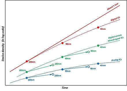
The most suitable manufacturing process node for mixed-signal IC design lags behind the bleeding edge of process technology, and the choice of nodes is a trade-off of several factors, which ultimately depends on the amount of analog and mixed-signal circuitry included in the device. More precisely, a more digital-centric mixed-signal design approach enables the designer to leverage more advanced process nodes in order to resolve one of the most challenging commercial issues with analog circuit integration – the ability to integrate analog to reduce cost while increasing functionality. Design engineering teams at many leading semiconductor companies are actively pushing the boundaries of mixed-signal design and trying to address this challenge with novel solutions in which logic gates and switching elements are replacing amplifying and bulky passive devices.
The IoT and mixed-signal design
The Internet of Things aggregates networks of IoT nodes, i.e., very low-cost, intelligent and connected sensors and actuators used for data collection and monitoring in myriad applications that improve energy efficiency, security, healthcare, environmental monitoring, industrial process controls, transportation, and livability in general. IoT nodes are projected to reach 50 billion devices by 2020, and possibly reaching the one trillion threshold just few decades later. These astronomic market numbers pose serious constraints in term of engineering, manufacturability, energy consumption, maintenance, and ultimately the health of our environment. In addition to being available in extraordinarily high quantities, all of these IoT nodes must be very small, energy efficient, and secure, and they are generally not easily accessible to consumers for maintenance. IoT nodes often must be required to operate with very small coin cell batteries for a decade or more, or possibly relying on energy scavenging techniques.
These application requirements make the IoT node the ultimate candidate for very advanced digital-centric mixed-signal design techniques. The ideal IoT node will require state-of-the-art mixed-signal circuits to interface to sensors and actuators. They must include RF connectivity, use very power-efficient wireless protocols and require minimal external components. They also must include power converters to optimize power efficiency and cope with different battery chemistries or energy sources, all characteristics generally obtainable with more mature process nodes. At the same time, these IoT nodes will require moderately complex, ultra-low-power computing resources and memories to store and execute applications and network protocol software, which is better addressed with finer technologies. The current instantiation of such a paradigm is a mixed-signal IC that is widely known as a wireless MCU: an easy-to-use, small-footprint, energy-efficient, and highly integrated connected computing device with sensing and actuating capabilities.
The proliferation of ultra-low-power wireless MCUs is critical to the advancement of the IoT. Wireless MCUs provide the brains, sensing and connectivity for IoT nodes, from wireless security sensors to digital lighting controls. The art and science of mixed-signal design is the key enabler for the development of next-generation wireless MCUs that bridge the analog, RF, and digital worlds and maximally leverage the power of Moore's Law, without compromises in performance, cost, size, or power consumption.
Alessandro Piovaccari is Vice President of Engineering at Silicon Labs.
Silicon Labs silabs.com @siliconlabs linkedin.com/company/silicon-labs opsy.st/SiliconLabsGooglePlus youtube.com/viralsilabs
Related Posts
.jpg)

Comments (4)
-
 Jessica MooreThis article about electronic components is well-written and informative. It covers a wide range of topics and provides valuable insights into the world of electronics. I found the explanations to be clear and easy to understand, even for someone with limited technical knowledge.November 30, 2019
-
 Adam TaylorI also enjoyed reading this article. It's great to see such clear explanations of complex topics. Looking forward to reading more from this author in the future.December 5, 2019
-
-
 Ryan FordI completely agree with the previous reviewer. This article is an excellent resource for anyone interested in learning about electronic components. I particularly appreciated the section on common types of resistors and how to read their values. Keep up the good work!December 5, 2020
Write A Comment
Popular News
-
Vishay Intertechnology, Inc. (NYSE:VSH) has been assigned a consensus rating of ...Jul 13, 2017
-
Vishay Intertechnology, a Rare Tech Stock on SaleThe valuation of technology sto...Apr 24, 2017
-
Digital and memory ICs constitute about two-thirds of today's roughly $320 billi...Jul 14, 2017
-
Integrated Circuit,Diodes, Transistors,Semiconductors,Capacitance,resistance,Tan...Sep 5, 2017
-
HELLA Aglaia and NXP open visual platform for automated driving safety....Sep 13, 2017